 Introduction
 |
What follows is several approaches to measure code speed and display it on 7-segment displays. Is one better than the other? That is for you to decide.
This page is about determining the speed at which your keyer is operating. But first, there are some words that I will be using and you need to know what I mean.
- The basic unit of the Morse Code system is the Element.
- A Dot is Element in length.
- A Dash is Elements in length.
- A Character is a sequence of dots and dashes that represents a letter, number, or puncuation character. (e.g. the sequence "⋅ –" is the letter "A", the sequence "⋅ – ⋅" is the letter "R")
- The space between the dots and dashes of a Character, is an Element.
- A Word is a sequence of Characters that forms a thought, idea, etc.. Each Character within a Word is seperated from the previous Character by 3 Elements.
- The space between the successive Words is 7 Elements.
| P = 11 Elements + 3 Elements |
| A = 5 Elements + 3 Elements |
| R = 7 Elements + 3 Elements |
| I = 3 Elements + 3 Elements |
| S = 5 Elements + 7 Elements |
| 31 Elements + 19 Elements = 50 Elements |
So this leaves us with the Element. If we define the length of a Element, we can define Words Per Minute, or WPM. The standard used to determine the length of a Element is the word PARIS. Actually, we will be using the word PARIS, plus the ending Word space (7 Elements). If we then calculate the number of Elements in this combination, we come up with exactly 50 Elements.
If we then send this combination (PARIS + Word Space) 5 times in 1 minute, we have sent at a rate of 5 WPM. Or 250 Elements per minute. If we then take 60 seconds and divide it by these 250 Elements we get 0.24 seconds/element. We can then say, at 5 WPM, each Element is 240 ms in length.
This can then be broken down into a simple formula for calculating WPM
based on the length of a single Morse Code dot.
WPM = dots/min/25 = 2.4 × dots/sec.
In the case of 1 WPM, the duration of a dot is 60 seconds / 50 dots per minute = 1.2 seconds per
dot. Also, for any other speed, we can define the dot length as equal to 1.2 seconds divided by
the speed in WPM. Based on the above we can use the following formulas:
Speed (WPM) = 1.2 / Dot length (Seconds) or
Dot length (Seconds) = 1.2 / Speed (WPM).
|
Digital Speed Control |
A digital readout for a keyer is nice. But because the oscillator that generates the dots and dashes is "keyed", and only runs when the key switches are closed, it's tough to get a stable display. Even with the front panel control, it's difficult to set the speed the same way twice. So here is a way to convert the speed control potentiometer from analog to digital.
The drawing shows the clock circuitry from the Heathkit HD-1410. The clock consists of transistors Q1, Q2, and their associated circuitry. When CLK_ENA is high, the clock (CLK_Q2) is disabled. Capacitor C3 charges through diode D1 and biases Q1 off. With Q1 off, the base of Q2 is high. Therefore, Q2 is also off and the clock output is low. Note that the high on CLK_ENA is also applied through D2 to IC4 pin 5. When CLK_ENA goes low (bit being sent), IC4A changes state. D1 is then back-biased and C3 begins to discharge through resistor R9, Speed control R101, and resistor R11. When its voltage drops to the base potential of Q1, Q1 begins to turn on. The collector of Q1 and the base of Q2 begin to go less positive and turn on Q2. As Q2 turns on, its rising collector potential is coupled through capacitor C4 to the base of Q1 and turns it on harder. Thus the condition is regenerative and happens very quickly.
So R9 and R101, the Speed Control, manage the clock speed. R101 is a 50K Ω potientiometer and R9 is fixed at 5.6K Ω. This sets the resistance range from 5.6K Ω (60 WPM) to 55.6K Ω (10 WPM), according to the manual. But the manual also says that, by changing R9 to 10K Ω, the speed range can be changed to 10 to 35 WPM.
Another suggestion is to add a 5.6KΩ resistor in series with R9 and then shunt Speed Control, R101, with a 33KΩ resistor. This is said to change the speed range to 8 to 35 WPM. Although, I have not verified it's operation. When R101 is set to minimum resistance, there will only be 11.2K Ω resistance in the circuit. That would correspond to the highest speed, and sounds about right for 35 WPM. But when R101 is set for maximum resistance, the 33K Ω parallel resistor would limit the maximum resistance of the combination to about 20K Ω.
Intuitively, that seems to be a little too low, to slow the clock circuit down to 8 WPM. Plus, the parallel resistor would modify the taper of R101. That may make it difficult to set a specific speed.
However, the intended point of this section is to come up with a way to be able to set the keyer to a known speed. One of the ways might be to replace the R101 with a switch selectable control. But a switch with a bunch of precision resistors, is not what I had in mind. Also, do you really need that kind of range? What about a nice incremental range from 10 to 26 WPM in 1 WPM increments.
|
Speed Demon, WPM display for Heath's HD-1410 Keyer - Jerry Wayne Campbell, K4ZHM |
The following schematic is for a Code Speed display system using CMOS ICs. I found this design in QST, November, 1982 by Jerry Wayne Campbell, K4ZHM. The unit described in the article was built directly into the HD-1410 cabinet, after the paddles were removed. However, it can easily be built separately and be modified to use with almost any keyer. The upper section of the schematic, U6, U7, U8, U9, is the keyer Clock Counter/Display. The lower section, U1, U2, U3, U4, is the 60 Hz Divider and Count Gate generator.
The Clock signal, for the counter, is obtained at Point D on the HD-1410 schematic. Point D is one side of the HD-1410 speed control that connects to the Anode of D3, as shown on the HD-1410 schematic.
The ICs used in this device are rather interesting. The counters used in the Clock Counter/Display (CD4026) and the Divider/Gate Generator (CD4018) are 5-Bit Johnson Counters. The CD4018s are unique in that, only the NOT outputs are used. This makes division by 10, 8, 6, 4, and 2 easily accomplished with a single feedback wire. Odd division can be achieved, but requires two of the outputs, for divide-by 9, 7, 5, and 3. But, since this device only requires two divide-by 6s and two divide-by 2s, interconnection is simplified. The CD4026 outputs drive Common Cathode LED displays directly.
The timing diagram below shows you how the 60 Hz clock divider (U1, U2, U3, U4, and U5) operates. The time, end to end, is 4.8 seconds or two complete count cycle times. These are the same signals shown in the original article. The signal on IC4-4 is the Gate signal for the counters, U6 and U7. When this signal is a "0", the counters will count. When the signal is a "1" the counter are inhibited from counting. So in the diagram, the counters are only allowed to count for 1.2 Seconds.
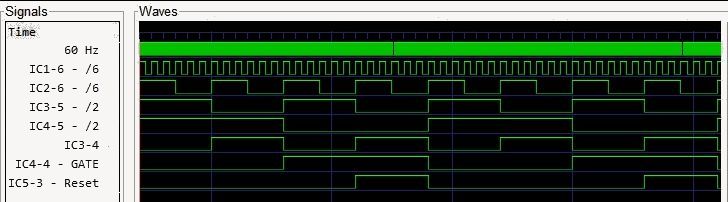
During the time that the Gate signal is a "1", the counter is halted, or Inhibited from counting. In that state, the LED displays, U8 and U9, should show the code speed in Words Per Minute (WPM). The Gate signal ANDed with IC3-4, produces the Reset signal, U5-3, for the counters. This happens at the end of each count cycle.
The clock in the HD-1410 starts and runs only when a dot or dash is being sent. So, at rest, the display should show "00". To set your speed, all you need to do is send either a string of dots or dashes. During sending, the speed shown on the displays will vary, showing you the average sending speed.
|
The Confidance Builder - a CW speedometer - Jim Hyde, WB4TYL |
The original article for this design was found in a September 1980 issue of 73 Magazine. I find this interesting because the author designed it so that you could key the CW Speedometer with a key or use some CW audio from your receiver.
This design uses the assumption that, when sending every day English by Morse Code, you tap the key an average of 2-1/2 times for each letter and 12-1/2 times for each average 5 letter word. Rather than counting the taps for one minute and then dividing by 12-1/2, this design counts the taps over a 4.8 second (60/12.5 = 4.8) time period.
This next drawing contains the Key Input, Audio Oscillator, Audio Input, Audio Rectifier, Schmidt Trigger, Pulser, and Power/Ground arrangement. The original circuit did not include bypass capacitors on the power bus. Bypass capacitors are commonly used to prevent the propogation of switching transients on the power bus. However, I have included some of them on the schematic as C9, C10, C11, and C12. The 0.1 µF capacitors should be connected directly across the ICs, from +5V to Ground.
For operation with a straight key, single lever paddle, or keyer, you should connected to the KEY input. This input is normally "high", with the keying device providing a ground. This is also the TRIGGER BUS. It keys the Audio Oscillator and is fed directly into the Trigger input on the Pulser (U3-NE555).
For operation from your radio, audio is connected to T1 and fed to a bridge rectifier (D1...D4). C3 filters the audio and R3 sets the Bias Voltage for triggering U1A, the Schmitt Trigger. T1 is a Audio Output Transformer used in reverse to step up the input voltage. If you have sufficient audio voltage, a interstage transformer (1:1) could be used. The output of the Schmitt Trigger also drives the TRIGGER BUS.
When the TRIGGER BUS is held "low", the Pulser is enable to oscillate. The
|
Digital Speed Readout for the Electronic Keyer - William B. Jones, W7KGZ |
This is another CW Speed Readout that was published in
QST, July 1978 by
William B. Jones, W7KGZ. It is based on the timing calculations that were presented at the top of
this page. Specifically the equation:
Speed (WPM) = 1.2 / Dot length (Seconds).
By sampling the keyer's clock signal, which is one dot in length, for 1.2 seconds, the counter section should be able to directly display th CW speed in WPM.
This is the keyer that was used with the readout QST, January, 1975 by James H. Fox, WA9BLK.
|
|