| CW Sendin' Machine by H. Alan Harp, K4PB |
each Schematic Page
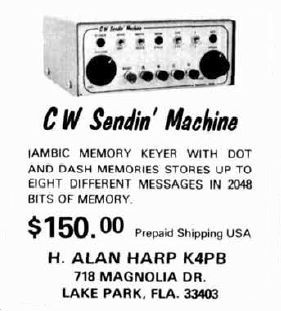
This is another keyer design. The thing that separated this keyer from the others, is that it was not published in any magazine. This keyer was manufactured and sold by H. Alan Harp, K4PB (SK March 18, 2020). And he made a lot of them. The schematic below is a redraw from H. Alan Harp's User Manual for his "CW Sendin' Machine". On the left is a advertisment from the September 1977 issue of Ham Radio magazine. It was pretty pricy for that time.
Initially, I scanned over the user manual and didn't see anything really exciting. The paddle input circuitry was common among many keyers, and there are only so many ways that you can include memory. So I thought I would just redraw the schematic and leave it at that.
| CW Sendin' Machine, Odd Configuration |
In the original schematic, gates were draw as gates. However, higher level logic, like Flip-Flops, Counters, and Rams were drawn as empty boxes with pin numbers. I did like the fact that K4PB used Demorgan Equivalents, with the gates, but the empty boxes took a bit of deciphering. As I was resolving some of the devices, I came across a SN7474 D-Type Flip-Flop (U15B on Page 2 below) that was configured oddly. On the right is a isolated drawing of that Flip-Flop.
- The PRE input is grounded.
- The Q output is wired back to the CLK and D inputs and used as a CLR signal on the other timing Flip-Flops (U16-A, U16-B, U15-A).
- Then a Keyer Clock (CLK) is applied to the CLR input.
- The Q is used to clock the RAM address counters.
| FUNCTION TABLE | |||||
|---|---|---|---|---|---|
| INPUTS | OUTPUTS | ||||
| PRE | CLR | CLK | D | Q | Q |
| L | H | X | X | H | L |
| H | L | X | X | L | H |
| L | L | X | X | H↑ | H↑ |
| H | H | ↑ | H | H | L |
| H | H | ↑ | L | L | H |
| H | H | L | X | Q0 | Q0 |
Now, I'm not sure I have ever seen a Flip-Flop configured that way. However, when I looked at the FUNCTION TABLE in the spec sheet, there is a entry that covers this configuration. I have listed the table from the spec, and then highlighted the entry in BLUE. This entry shows that when the PRE and CLR are both held "LOW", the Q and Q outputs both go HIGH.
There is a note on this particular state, that this configuration is nonstable and the output levels will not persist when either PRE or CLR returns to it's active (HIGH) level. But that is what we are counting on. If the CLR return to a HIGH level, as shown in the PINK highlighted entry, the Q will go LOW. So if we toggle the CLR from LOW to HIGH, the Q will toggle in the reverse.
| CW Sendin' Machine, User Manual |
ANSWER TO THE MOST FREQUENTLY ASKED QUESTION OF NEW OWNERS
The CW Sendin' Machine, when turn on with the switch in the READ position may conme on key down. This is due to the fact that random data is in the Memory until good data is written into it. Setting the switch to WRITE will correct the key down problem. The same is equally true when turning the switch from one Memory to another for the first time since turn on.
A power crash may cause the unit to lose its Memory and come on key down also.
it is O.K. to leave the unit turned on all the time, but do not leave it connected to a rig with VOX ready to go or a power crash may leave you key down creating QRM and damage your rig.
UNPACKING INSTRUCTIONS
Carefully unpack the CW Sendin' Machine. There should be a package containing three cables. The TV cheater cord is for AC power and connects to the mating socket on the back. The three conductor cable is for connecting to the paddle. The clear insulation wire is ground. The red is the dah wire, the black is the dit. The cable with the miniature phone jack and phone plug connects from the miniature phone jack on the back to the key jack on your transmitter.
There are two key jacks on the back of the CW Sendin' Machine. Looking from the back, the one in the upper right corner is for keying positive keyed transmitters such as Drake TR7, ICOM 701, Ten Tec, Atlas, etc. The one in the lower left next to the paddle plug is for grid block keying such as the Kenwood TS520, or most transmitters with tubes in the final stages.
Connect the power cable and paddle to the unit.
OPERATION
Set the toggle switches as follows:
- SPKR, WRITE, 256, and 1.
- Connect the power cord to an AC outlet.
- Turn power on, (switch on the volume control).
Start sending with the paddle. Adjust the speed control to a comfortable speed. The POWER CYCLE LED will light and remain lit as long as the memory is cycling. As long as it is lit, your message is being stored in memory. If it goes out before you are finished with your message, it is too long for a 256 bit section. After you have finished your message, wait until the MEM CYCLE LED goes out.
It is important to start sending immediately after depressing the button. Any delay will be evident on play back.
To send the stored message, set the switch to READ, Depress A. The message you have just stored will be sent automatically.
Similarly, messages may be stored in other section of the memory. Stored messages will remain and can be sent again and again until another message is written in the section on memory or the power is turned off. For this reason, you may want to leave your keyer on all the time.
Depressing the RESET button will cancel a memory cycle inprogress. Reset may also be accomplished with the switch in the READ position by operating paddle. After any reset, another memory cycle may be started immediately. Our automatic reset feature allows you to interrupt one message with another simply by pressing anotther buyyon. A message may be started over by pressing the button again.
If, when writing a message to memory an error is made, you may reset and start over without waiting for the cycle to complete. If you do not wish to resend the entire message, you may start the cycle in the read mode, allow it to run to a point just prior to the error, then quickly set the switch to WRITE and complete the message while the cycle continues.
To use memory #2, simply se the switch to 2. Repeat the same procedure used with memory #1 Actually, there are eight 256 bit sections of memory available to store message in.
DOT AND DASH MEMORIES
The feature can be demonstrated as follows:
- Set the keyer to its lowest speed.
- Close first the dah paddle then the dit.
- Quickly release both paddles before the dah completed.
You will note that the dah does complete and the dot follows. The opposite can be demonstrated by closing first the dit then the dah paddle and releasing before the dit completes. This feature allows the paddle to be one dit or dah ahead of the keyer.
IAMBIC OPERATION
Using a dual lever paddle, note that if both contacts are closed, alternates between dits and dahs. Of course it makes first whichever was closed first. If both levers are operated during a dah, a dit will follow and vice verse. Using this feature, the C, R, K, F, L, Y and Q can be sent with fewer finger motions than with a single lever paddle. For instance:
- To make a C, close first the dah then dit paddles. Open them both during the second dah.
- To send an F, close the dit lever and tap in the dah during the second dit.
- To make a K, close the dah then the dit, release both during the dit.
- To make an R, close dit, tap the dah during the first dit, release the dah during the last dah.
- To make an L, close the dit and tap the dah during the first dit, release the dit during the last dit.
This method may be difficult to become accustomed to if you have already learned the other way. However, it can be easier once learned and may allow you to send faster once you have mastered it.
| CW Sendin' Machine, Page 1 - Keyer Logic |
| CW Sendin' Machine, Page 2 - Keyer Timing |
| CW Sendin' Machine, Page 3 - Memory Timing/Control |
| CW Sendin' Machine, Page 4 - Memory/Tone Generator |
Note that the address lines (A00 throu A09) going in to the RAMs (U1 and U3) do not match the address labels. I adjusted these addresses to correspond to the original schematic in the User Manual. In the end, it makes no difference as to the order of the address lines. Address lines were often swapped around to make printed circuit layout easier.
| CW Sendin' Machine, Page 5 - Power/Ground |
| CW Sendin' Machine, Page 6 - Chassis Wiring |
| CW Sendin' Machine, Page 7 - Automatic Reset/Keying Interfaces |
The Automatic Reset Feature was added after the PCB of the CW Sendin' Machine was created. The feature was created on a small auxilliary PCB and mounted on top of the original board. The auxilliary board covered U11, U12, and U13, and was connected to the main PCB via short bare wires. The inputs to the board only connects to the switches for RESET, A, C, and D. Pressing switch B would automatically close switch A and C, via CR1 and CR2.
The Grid-Block Keying interface is the default keying interface. This type of keying is usually on older tube or hybrid radios. It's characteristic is a high negative voltage on the keying pin. The transistor Q1 needs to be rated higher than the keying voltage. There are two inputs to the interface. The TUNE input comes from the tune switch which is normally in the closed position. Then open, Q2 is saturated and the collector and R14 will go to ground. R14 going to ground will cause the KEY LED to light and will key the radio through Q1. When the TUNE switch is closed, the interace is driven by the CODE_OUT. When the dit and dah paddles are idle, and the unit is not playing back a message, CODE_OUT will be low. A high on this input indicates that a morse element (dot or dash) is being sent.
The Positive Keying Output circuit is a bit undefined. In the original manual there are no assigned Reference Designators, the input doesn't appear to be correct, and the output is assigned to an already used pin. I can only assume that this was not part of the original design. The input is listed as comming from the collector of Q5 (Page 2). But that's the collector of one of the dot oscillator transistors. It would simply turn on/off at the dot rate. The input should be the same signal that the Grid-Block Keying interface uses. I adjusted the output pin to an unused pin here and on Page 6. This interface also does not include activation via the TUNE switch.
If you only need the Positive Keying Output circuit, you still need to include the Grid-Block Keying interface to light the KEY LED unless the whole interface is redesigned.
| CW Sendin' Machine, Page 8 - Component Layout |
The original CW Sendin' Machine was built on a PC Board that had a dual connector at the bottom. The left side of the connector had 16 pins and the right side had 14 pins. I assume that this is for "keying" purposes, so that the board can not be plugged in backwards. While not shown on the schematic pages, Pins 1 through 31, and 60, are ground.
The drawing below is a free hand rendering of the original circuit board. The ICs are fairly close to their postions and the connector accounts for all of the signals listed in the drawings. My guess is that the circuit area is about 7-1/2" wide by 3" high. The board was positioned with the connector end facing the rear of the chassis. The pictures that are available to me, do not show where the power supply was mounted except for the fact that the regulator was mounted at the center of the rear panel.
Note that capacitor C7, which is the Dot Clock timing capacitor, is 1.0µF/50V non-polarized mylar.
| Original Schematic Errors or Oversights |
This is a list or Errors or oversights that show up in the CW Sendin' Machine User Manual. There is far more than I expecte ,but then, the schematic is hand drawn and seemingly not used for PCB layout.
- On all sheets, ICs are empty boxes, with only pin numbers to aid in deciphering their function.
- Inconsistant use of wire connection dotting.
- Inconsistant drawing of ICs. Gates are drawn going right, left, up, and down. D-Flops are shown differently on different pages.
- On Sheet 2, U1 has pin 13 listed twice. It is correct in the drawings above.
- On Sheet 2, R16 is listed twice. Once, connected from MEM_SEL (53) to +5V and again on the output of U8-12 going to MEM CYCLE LED (44).
- On Sheet 2, R23 is listed twice. Once, connected from C (49) to +5V and again connected from D (45) to +5V.
- On Sheet 2, U3 lists pin 9 as one of the address pins. Pin 9 is the VSS (Ground) pin. The correct pin number should be 7. It is correct in the drawings above.
- On Sheet 2, U5 lists pin 2 twice. The wire that is tied to pin 1 should be connected to pin 12.
- On Sheet 3, An input from U12-3 is shown. That incorrect and should be U12-8.
- Reference designator R23 listed twice. Changed to suite drawing.
- The Positive Keying Output Circuit shows the input comming from the Collector of Q5 and the output going to pin 46. But the Collector of Q5 is just the keying oscillator and Pin 46 is already used by the "A" switch. There is no explanation of it intended use, however, I assume it was intended for the keying of radios that have a positive low voltage (~+5V) and are grounded to key the radio.
- In the description to create a R, Iambically, the dit and dah are reversed. I corrected it in the text.
- The Automatic Reset Feature drawing shows the input pins for U18 incorrectly. One section of U18 lists pins 1, 2, 3, and 4. However, the correct pin list should be 1, 2, 4, and 5.