| The Accu-Keyer, by James M. Garett, WB4VVF |
| The Accu-Keyer Features |
|---|
| Self-completing Dots and Dashes |
| Dot and Dash Memories |
| Iambic Operation |
| Dot and Dash Insertion |
| Automatic Character Space |
| 5-50 WPM Speed Range |
| Low Cost |
Probably, one of the keyers that has seen the most print, is the Accu-Keyer, by James M. Garett, WB4VVF. This keyer was initially published in the August 1973 issue of QST Magazine, and it was a big sensation. Over the years, the Accu-Keyer has seen 20 or 30 articles directly addressing the Accu-Keyer. Some of those articles were just add-ons, like a side tone generator or a keying alternative. But some of the articles were fixes for inherent problems with the keyer.
The original was designed with standard SN7400 series ICs. However, Gene Hinkle, WA5KPG, came up with a CMOS (CD4000 series) version in the August 1975 issue of 73 Magazine. The two versions are mostly identical. The CMOS version was aimed at the QRP crowd, but could be used by anyone. You just had to be careful, because CMOS was sensitive to external fields.
The Accu-Keyer design also appeared in the 1979 issue of the ARRL Radio Amateurs Handbook (56th Edition). It is important to note that there is an error in the schematic. However, it looks like the printed circuit board for the Accu-Keyer is correct. On earlier pages, in that same handbook, there is information on the Accu-Memory that includes a led message display.
So I thought it might be interesting to look into the original design and some of the upgrades. I could readily build an Accu-Keyer and poke at it with my oscilloscope. But I thought it would be more informative, and easier to experiment with, if I wrote a Verilog simulation. Since the keyer is not a imbedded microprocessor, it isn't that difficult. So I did. But to be clear, I only included the keyer logic. Trying to include the side tone generator or keying circuitry wouldn't be productive.
Note, I am not going to go into a detailed explanation of the keyer circuit. I will keep my discussion relatively high level. I you need a detailed explanation, obtain a copy of the original article from the link in the first paragraph. It is also available on various web sites. A simple Google search should be all you need.
Also note that in the web page on CW Speed, is a digital speed readout for the Accu-Keyer.
| Accu-Keyer Block Diagram |
Below is a redraw of the Block Diagram for Accu-Keyer. The diagram shows the general flow of the keyer logic. Each block is annotated with the IC reference designators to make it easier to follow the schematic and the timing diagram.
| Accu-Keyer Timing |
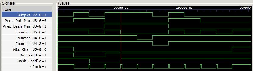
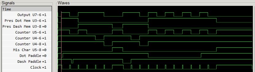
Below is a redraw of the Timing Diagram for the Accu-Keyer. The quality of the copy that I have is pretty bad in places, so I recreated the timing diagram as best I could. The diagram show 20 clock periods of the keyer and basically reads from the bottom to the top. All action starts with the tap of the Dot Paddle, at T1, for the start of the letter A, T1 → T6. T6 → T9 is the space between two letters. You can see that, even though the Dash Paddle is closed prior to T9, the Auto Space insures that the Dash is not started until the correct spacing is achieved. You could close the Dash Paddle later than T9. But all that would do is increase the space between letters. T9 → T18 is the sending of the letter B. T18 → T21 is the space after the letter B.
| Accu-Keyer Simulation |
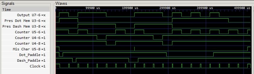
If you adjust the simulation stimulus (that is the dot/dash paddle times) to that of the timing chart above, the simulation output exactly matched the original article. The image below is taken from the output of the simulation. I aliased the signals so that they match the original. As with the original timing diagram, the simulation sends the letters A and B and Auto Letter Space is enabled. The total simulation time from the start, T1, to the end, T21, is 0.5 seconds. This is effectively a rate of 48 WPM. The speed is changed simply by changing the duration of the Clock. However, changing the speed would not change the timing relationships.
| Accu-Keyer Schematic |
-
Printable Images of each Schematic Page
- Page 1 - Keyer Timing
- Page 2 - Paddle Input and Dot/Dash Memory
- Page 3 - Output and Power/Ground
What follows is the schematic for the Accu-Keyer. I split the keyer schematic into three logical sections. You may notice that the schematic looks a little different than the original schematic from the QST article or the Handbook. That's because I have some very definite notions on how a schematic should be drawn.
| Accu-Keyer Modifications |
The schematics above, are the Accu-Keyer as it was originally presented. But shortly after the initial publication, feedback from the users/builders was starting to pour in. Several of them are listed below.
| Accu-Keyer Speed Readout |
-
Printable Images of each Schematic Page
- Page 1 - Speed Readout Timing
- Page 2 - Speed Readout Counter/Display
- Page 3 - Speed Readout Power/Ground
This is a design by Bill Wageman, K5MAT and was in Ham Radio Magazine, September, 1979. The descriptions below are directly out of that article. I redrew the schematic with a bit more detail, to make it easier to understand. I adjusted the description to account for any modification I made to the schematic. Some of the parts did not have Reference Designators. I added them as I saw fit.
| Page 1 - Speed Readout Timing |
The logic diagram for the Speed Readout Timing is given in schematic Page 1. U1 and U2 are 556 dual timers. One half of U1 generates the high-frequency pulses, available from pin 5, that form the basis of the clock/readout. The other half of U1 is the time base for the display counter, with the output on pin 9.
R1 is the speed control and is mounted on the front panel of the keyer. C1 must be a reasonably stable capacitor (Mylar), not one of the ceramic bypass types. C1 and R2 determine the maximum keying speed, and the value of Rl determines the range. The value of R2 will probably be between 6,000 Ω and 22,000 Ω for a 50 WPM maximum, and may be selected for this purpose. If C1 is changed for any reason at some later time, it may be necessary to change R2 to bring the maximum speed back to the one desired.
R3 is mounted on the printed circuit board and is used to adjust the 100-ms time base for the display counter. If it is not possible to adjust the "on" time at pin 9 of U1 to 100 ms, it may be necessary to change the value of R4 to bring the pot within the proper range. C2 is the most critical component in this entire circuit.
U2 is simply a sequential timer. The trailing edge of the 100-ms counter gate triggers a pulse of short duration at pin 5 of U2. This pulse, after inversion by U5C, strobes the count in the decade counters into the display. It also triggers another short pulse, at pin 9 of U2, which is used to reset the counters to zero, preparing them for the next update.
| Page 2 - Speed Readout Counter/Display |
The logic diagram for the Speed Readout Divider/Counter is given in schematic Page 2. U3, a 7490 decade counter, and U4, a 7492 duodecimal counter, form the divide-by-120 divider that generates the clock pulses for the keyer logic. This divider is gated on and off by the inhibit line from the keyer, with the inhibit signal resetting the divider to zero and holding it there when all keyer action is complete. Inverter U5B ensures that the clock pulses have the right polarity for the Accu-Keyer, and might not be necessary in other keyer designs. This cornbination forms a keyer clock which is always within 1/120th of a dit of starting, a negligible delay at any speed.
U5A controls the display counting. The pulse generator pulses are fed to the counter only when pin 9 of U1 is high. When it is high for precisely 100 ms, exactly one tenth of the pulse generator frequency is counted. U6, another 7490 counter, is for the Least-Significant-Digit (LSD) and, by including it without display, the jitter inherent in this digit is eliminated. This results in a stable display considerably superior to using only two decade counters with a 10-ms time base. U7 and U8, both 7490 counters, are the actual display counters, with U8 serving as the Most-Significant-Digit (MSD) counter.
The displays themselves, U9 and U10, are easy to use, with an attractive, bright display, although they are a bit expensive. Other displays may be substituted, but it might be necessary to incorporate data storing latches, which are built into the 5082-7300 displays. A nonblinking display is a necessity, so be sure to add latches if they are not in the displays you choose.
Connection to the Accu-Keyer is really quite simple. CR1 in the original Accu-Keyer clock must be removed from the circuit. A wire is connected to the vacated hole at the anode end for connection to the inhibit line in the new clock. The foil should be cut as indicated in fig. 2 and the old speed control wires should be removed. The clock line may then be conmected to the vacant hole near the cut in the foil. Connect VCC and ground both the readout and the clock board, and you're in business. You may wish to remove the old clock components from the Accu- Keyer board, but that is not really necessary.
I have not included a power supply, since most will be able to use the supply in the Accu-Keyer. It might be necessary to increase the size of the input capacitor ahead of the regulator to keep the voltage high enough to maintain regulation. If your supply is incapable of providing the necessary current, any standard 5-volt power supply design will be satisfactory.
Full-size board layouts and the component placement diagram are shown in figs. 3 and 4. They are single-sided boards, and should be easy to duplicate by those who wish to roll their own. There is no reason why point-to-point wiring cannot be used, since the layout is not critical.
| Page 3 - Speed Readout Power Ground |
| Trailing Dits |
Trailing Dits - Tony Berg, W1OT, wrote an article in the October 1994 issue of Morsum the Magnificat, the Morse Magazine, page 18. The article was on keyer designs that have a "Auto Character Space" feature and/or a "Dot/Dash Memory" feature. The Accu-Keyer fit right into that catagory. The original article has more detail than I will be providing, and is a recommended read.
In the article, W1OT makes the point that, with a keyer it is possible to generate sloppy characters or characters with unwanted training dots. In particular, this is with keyers that have an "Auto Character Space" feature and/or a "Dot/Dash Memory" feature. An example might be sending the letter "A". To send the letter "A" you must close the dot paddle followed by the dash paddle. Then, you then must release the dot paddle before the dash starts. Otherwise the "Dot/Dash Memory" will record another dot which will be generated after the dash making the "A" a "R". At slow speeds, that's not an issue. But at higher speeds, the release time becomes smaller and smaller.
The drawing on the right is the "fix" for the Trailing Dots on the Accu-Keyer, that was published in QST, July 1978 by Ronald Hanthorn, K8AW (Bottom of page). I changed the reference designators (U1, U2 ⇒ U8, U9, respectively), shown in the QST article. This was to eliminate any confusion with the Accu-Keyer schematic. The modification is designed to eliminate the trailing dot, but maintain dot insertion for such letters as K. When implementing this fix, the Dot-Input lead of the keyer should be disconnected from the key jack and wired to the output U9B, Pin 6.
I also found this fix in a document titled "Accu-Keyer Manual". The document was a bit crude and contained a schematic of the Accu-Keyer and a different layout than the original. The Trailing Dot Fix was scribbled in at the end. But, that drawing had a different signal going into U2A Pin 1.
| Weight Control |
Another modification is the addition of Weight, that was published in QST, February 1978 by Hal Kennedy, N4GG. The article did a good job of describing the modification and why it might be needed. But the artical skipped the detail on exactly where the bottom terminal connects. The article only says "back to the clock-speed-determining components". Aren't most of the components in the oscillator, clock-speed-determining components?
However, the lack of detail was handled in the Feedback section of
the next issue of QST. In the update it said:
The weight-control drawing appearing in "Hints and Kinks" for February, 1978, should have indicated
that the 47KΩ resistor is to be connected to C1, R4, CR1, and Q1.
The schematic on the right has been adjusted.
| Sidetone Oscillator I |
The original Accu-Keyer article did not include a Sidetone Oscillator. But adding one is relatively simple. On the right is the schematic of one Sidetone Oscillator, suggested by Hal Morris, W4VUO/3, in the June 1975 issue of QST Magazine. Hal used the same TTL logic as used in the original Accu-Keyer. The input for the sidetone comes from the CW_OUT signal on Page 1 of the Accu-Keyer.
| Sidetone Oscillator II |
This sidetone oscillator was published in the 1976 Radio Amateur Handbook, Page 365 along with the schematic of the original Accu-Keyer, Accu-Memory, alternate power supply, and Cathode Keying circuit. Below is a quote from the article.
Should a keying monitor be desired, the diagram on the right may be used to construct a circuit which will afford plenty of volume and stable pleasing tone. The circuit is a modified version of the code-practice oscillator appearing in Chapter 1. Equipped with such a monitor, the Accu-Keyer becomes ideal for conducting code practice sessions for small and medium-sized groups.
| Power Supply |
The original "Accu-Keyer" had a very simple power supply that ran from 8 to 10 VDC or 6.3 VAC. It consisted of a 1/2 Amp Rectifier Diode, a 5.1 Volt, 0.5 Watt, Zener Diode, a dropping resistor (27 Ω), and a couple of Electrolytic Capacitors (2,000 µF and 50 µF). This was pretty convenient as many transmitters of that era provided access to the 6.3 VAC filiment transformer. You could also run it directly from a 9 VDC battery, as long as you remembered to disconnect the battery when it wasn't being used. Otherwise, the circuit would drain the battery in a relatively short time.
If the intent is to include the Accu-Memory upgrade, you will probably need a better power supply. Above is a schematic for other possible power supplies. The first one (Power Supply #1) uses a 12.6 VAC transformer with a center tap. The transformer feeds two diodes who's output goes to a 2,000 µF Electrolytic capacitor and a LM7805 Regulator.
The second power supply (Power Supply #2) uses a transformer without a center tap that feeds a four diode bridge rectifier. This should provide the regulator with a slightly higher voltage than Power Supply #1. It shows a LM309K regulator but can easily be used with a LM7805 Regulator.
| Output Keying |
It is important to know the keying characteristics of the transmitter you are keying. The Accu-Keyer output circuit was designed to only drive transmitters using Negative Grid-Block keying. The transistor specified, 2N4888, should withstand -100 volts when turned off. Older tube type transmitters often used Grid-Block keying which can develope more then 100 volts (negative) across the keying terminals. The voltage across the transmitter's keying terminals should be measured first. This voltage should be negative and in the range of -50 to -150 volts.
The diagram on the right is an alternative keying circuit, for use with newer transmitters that use Cathode Keying. Both types of keying can be included by providing separate outputs for each one. Just make sure they are clearly marked.
| Keyer Oscillator |
Normal operation of the Accu-Keyer
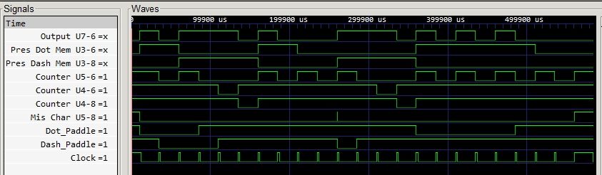
This next simulation has the same dot/dash paddle operation as the previous simulation, but the "Auto Character Space" switch is "closed", disabling the "Auto Character Space" feature. You will notice the space between the last element of the "A", the dash, and the first element of the "B", is much smaller. This is because the keyer is no longer controlling the space between characters. You might also notice that the dash is "short".
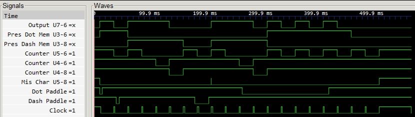
In this next simulation, I only show the generation of the single character "A". But the character that is actually generated is a "R". This is because I changed how the dot and dash paddles are activated in the first simulation. In this simulation, the dot paddle is closed followed by the dash paddle. This is a squeeze operation that you might use when sending. But the dot paddle is not released until the dash output starts. The actual time shown is only 60 us after the dash starts, but that is more than enough to cause the keyer to generate a trailing dot. This turns the "A" into an "R".