| ICKEY by Frank Van Cleef, W1WCG |
About a year after the Micro-TO Keyer, by Chet Opal, K3CUW, came out, Frank Van Cleef, W1WCG, came out with a keyer that contained Dot and Dash memories. It was a good design, but with innovation comes problems. W1WCG's design was published in QST, November 1968 .
As with the Micro-TO keyer, the ICs are old obsolete RTL (Resistor Transistor Logic), but they are from a different series produced by Motorola. In a few places, the gates are employed as inverters rather than logic gates. This is a common practice. Rather than add an extra package, and have gates and inverters left over, the extra logic gates are pressed into service as inverters. You might also notice that several of the MC724Ps are drawn differently than the others. Specifically, U1-A, U1-D, U2-A, and U2-D, and U3-D. The basic MC724P gate is a NOR gates. What is shown on the schematic is the DeMorgan Equivalent. This helps me understand the circuit. I have also added some logic level markers to note the idling states.
Of interest might be the capacitor marked C3, in the center of the drawing. The keyer's CW OUT is fed back to the input of U4-B. Then both the CW OUT and CW OUT are fed to the DOT RESET and DASH RESET gates. The capacitor provides an increased capacitance load which increases the propogation delay through U4-B. That extra delay produces a longer reset pulse.
Note that I have modified the Reference Designators. The original drawing had some of the parts assigned Reference Designators and some not. IMHO, all parts should have a Reference Designator.
In the upper right corner of the keyer drawing, Page 1, is the Keyer Clock circuit. To add Weight Control, the Keyer Clock circuit requires modification. On the right is a schematic showing the original Keyer Clock, modified for Weight Control.
In the schematic, C11 is substituted for C4, and R3 is removed. R4 is then reconnected as shown. R14 is a 250Ω Linear control. CR7, CR8 are any small silicon diode. The X and Y inputs, on the left of the schematic, come from the DOT GEN flip-flop (U5-A), on page 1 of the keyer schematic.
Again, the Reference Designators have been adjusted for clarity.
Simulation
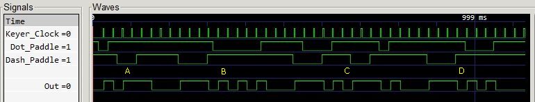
The simulation output below shows the ICKEY keyer generating the letters A, B, C, and D. The keyer does a good job of generating good element lengths and element spacing. The simulation even makes the space between letters look good. But that is not specifically a keyer feature. The simulation was carefully crafted to provide the proper letter space. It is up to the user to create the proper letter and word spacing. Meaning that, a user could easily run all his letters and words together.
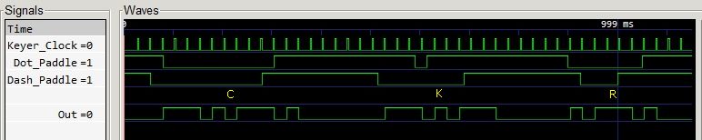
An advantage of having a simulation is that, complex synarios can be tried. So I tried operations like, strings of dots or dashes, just holding a paddle closed. I also tried closing both paddles. This produces alternate dots and dashes. The start element is determined by which paddle gets closed first. I was even able to try inserting one element, while holding the other element paddle closed. The letter "K" is an example. The dash paddle is held closed and the dot paddle is tapped. This produces the letter "K" with very little effort. Below is and example of "squeezing" out the letters "C", "K", and "R". Of course, "squeeze" keying takes a bit of practice.
Also visible from the simulation is the fact that the keyer clock runs continuously and is asynchronious to the paddle closures. The user has to get in sync with the clock. That really shouldn't be difficult to do. However, at lower speeds, sending may seem a little choppy. Overall, use of this keyer will take a little practice. The keyer does everything is was designed to do and works as advertised.